
A technical and legal examination of Micron Technology, Inc. v. BeSang Inc. (Fed. Cir. Oct. 30, 2026): the architecture, the prior art, and the words that decided validity
Case facts |
|
Decision | Micron Technology, Inc. v. BeSang Inc., Nos. 2025-1320, 2025-1377 (Fed. Cir. Oct. 30, 2026) (nonprecedential) |
Panel | Lourie (author), Reyna and Hughes, Circuit Judges |
Patent | US 7,378,702 B2, “Vertical memory device structures”; inventor Sang-Yun Lee; owner BeSang Inc. |
Proceedings below | IPR2023-00900 (Micron), final decision Nov. 13, 2024; IPR2023-00991 (Intel), final decision Dec. 11, 2024 |
Claims | 1 and 13–17; all upheld |
Prior art | Six references: Watanabe, Lee Patent, Lee Application, Aspar, Kim, Park |
Result | Affirmed: the claims were not shown to have been unpatentable |
1. The case in brief
Two of the largest memory and processor makers, Micron and Intel, challenged a 2004 patent on stacked vertical memory. They used six prior-art references across six obviousness grounds. Every ground failed, and each failed at one specific point: a bonding temperature that would destroy the structure, one missing claim element, or a structure that was close but did not meet the claim’s words.
This article explains the technology from the patent itself. It then compares the patent with each prior-art reference in drawings and maps every ground onto the claim elements. It closes with the legal reasoning and with drafting lessons for attorneys.
2. The architecture: memory bonded above finished logic
The ’702 patent starts from a limitation of conventional chips. Integrated circuits “contain transistors that are primarily implemented on a single major surface of a substrate,” and these lateral devices “consume significant amounts of chip area.” Memory arrays and their control logic therefore compete for the same silicon surface. Each step of lateral shrinking has become more expensive.
BeSang’s answer is to move the memory cells off the surface. They are built vertically in a thin, separately made single-crystal layer that is bonded on top of a wafer whose logic and wiring are already finished.
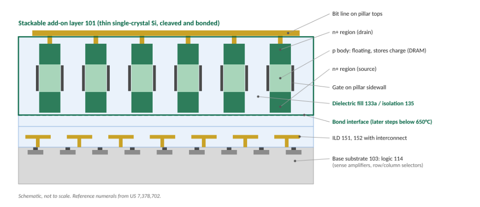
Figure 1: The ’702 structure in cross-section. A stackable add-on layer (101) of vertical n+/p/n+ pillars separated by dielectric fill (133a) is bonded above a base substrate (103) whose logic (114) and interconnect (ILD 151, 152) are already complete.
2.1 How the structure is made
- Donor layer. A separate single-crystal wafer is doped into a vertical stack of layers. Before bonding it is “unpatterned” and has “only a vertically oriented stack of layers.”
- Bond. A “relatively thin, single crystal portion of a semiconductor wafer” is “cleaved and bonded to another previously fabricated wafer.” Because it has no lateral features yet, it “could be transferred along with a simple notch alignment.”
- Form the cells. Individual structures are formed “by etching through portions of the doped stack to electrically isolate those structures.” “The spaces between such individual structures may be filled with dielectric material” to re-form a layer “without gaps or voids.”
- Stay cool. Gate-dielectric processing is limited to “process operations at temperatures below 650° C,” and films “requiring processing at temperatures more than 650° C” are excluded. Unlike conventional MOSFETs, where “a high temperature heat activation operation is required after the source/drain ion implantation,” “the FLD architecture does not require a high temperature process.”
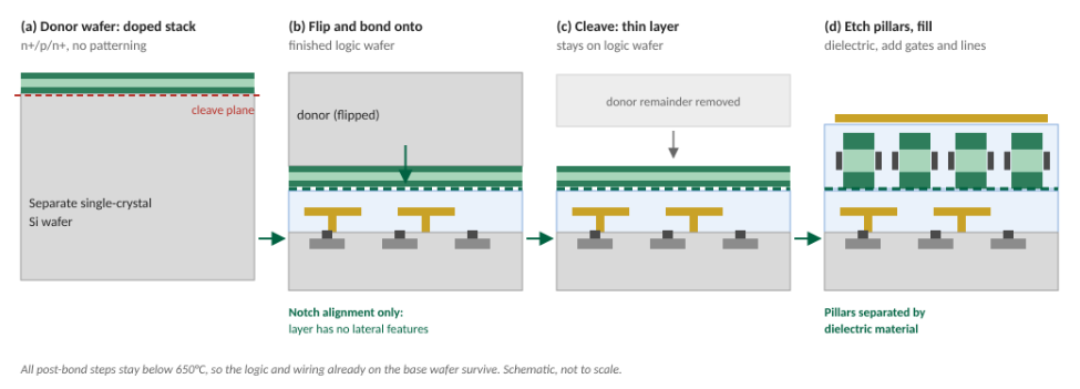
Figure 2: The ’702 process. Doping happens before transfer, so no high-temperature activation is needed after bonding and the logic below survives.
2.2 Cell types the patent discloses
Cell type | Implementation in the ’702 patent | Claims |
DRAM | Vertical n-type enhancement MOSFET; with a floating body “electric charge is temporarily accumulated in the body (p-region)” (FIG. 8). Alternatively a capacitor on the pillar or in the base or ILD: MIM, PIP, MIP or trench (FIGS. 2, 8–11). | Claim 1 |
SRAM | Negative-differential-resistance devices: thyristor, charge-trapping MOSFET, p+/GeSi/n+ tunnelling diode (FIGS. 14–22) | Not asserted |
Nonvolatile, dual gate | Floating gate 123k with control gate 123 on an SOI pillar (FIG. 23) | Claims 13, 14 |
Nonvolatile, charge trap | ONO charge-trapping gate insulator 183g with a gate (FIG. 25) | Claims 13, 15 |
NAND string | “Four vertical memory cells with serial connection”, described as possibly “part of a NAND architecture flash memory product” | Claims 16, 17 |
2.3 Technical advantages stated in the patent
- Higher density without smaller lateral features; shared bit lines or dual-port cells give “a factor of two” density increase.
- Memory and logic are each made in their own optimized process, then stacked, avoiding difficult system-on-chip process merges.
- High-k gate dielectrics and metal gates become usable because no high-temperature activation follows.
- Graded channel doping is possible, which may reduce short-channel effects.
- No “shadow effect” from angled implants into tall pillars, because doping precedes patterning.
- Defects on the cleaved surface have “little impact” on gate oxide, since that surface is a heavily doped source/drain region.
- Lower contact-resistance voltage drop than lateral devices; redundant cells can replace defective ones.
3. The claims: the words that were tested
The Federal Circuit treated claims 1 and 13 as representative (’702 patent, col. 10 ll. 47–63; col. 12 ll. 24–34).
Element | Claim 1 (DRAM) | Claim 13 (nonvolatile) | Decisive in |
Base | “a substrate having electrical devices formed therein, and further having at least one dielectric layer and at least one interconnect layer disposed above the substrate” | [13a] “a substrate having electrical devices formed therein, and further having a dielectric layer disposed above the electrical devices” | Micron (heat limits) |
Memory layer | “a first stackable add-on layer … including a plurality of vertically oriented semiconductor memory cells disposed within the first stackable add-on layer” | [13b] “a stackable add-on layer having a plurality of vertically oriented semiconductor memory cells” | Intel, claim 13 |
Separation | “the plurality of vertically oriented semiconductor memory cells separated from each other by dielectric material” | — | Intel, claim 1 |
Bond | “bonded to a layer of the substrate that is the greatest distance from the substrate as measured from the bottom surface of the substrate” | [13c] “the stackable add-on layer being bonded to the dielectric layer” | Micron |
Cell type | “the memory cell is a DRAM having at least one transistor” | [13d] “the memory cells are nonvolatile memory cells having at least one transistor” | PTAB alternative ground (Micron) |
Dependent claims 14–17 add a floating gate with a control gate on an SOI pillar (14), a charge-trapping gate insulator (15), at least two serially connected nonvolatile cells on one SOI pillar (16), and a link through an interconnect line on a dielectric layer to a cell on a second pillar (17).
4. The prior art at a glance
Reference | Number, owner | Date | What it discloses |
Watanabe | US 5,091,762; Toshiba; inventor Toshiharu Watanabe | Priority July 5, 1988; issued Feb. 25, 1992 | Stacked “conductive planar members” with wires passing through them; a one-bit cell (MIS FET + capacitor) at each crossing. In the “stacking method” the members are “bonded together” by a “thermal process of 900° to 1000° C.” Peripheral circuit and transistors in the substrate. |
Lee Patent | US 6,881,994; Matrix Semiconductor (later SanDisk; now Woden Technologies) | Priority Aug. 14, 2000; issued Apr. 19, 2005 | Monolithic 3D array of charge-storage TFTs. “Layers of each level of the array were directly deposited on the layers of each underlying level.” CMP between levels gives flatness “on the order of 4000 Angstroms or less.” Drivers (sense amps, charge pumps) in the monocrystalline substrate. |
Lee Application | US 2002/0028541 A1; same application (09/927,648) and inventors as the Lee Patent | Filed Aug. 13, 2001; published Mar. 7, 2002 | Pre-grant publication of the same Matrix disclosure: polysilicon pillar TFTs (N+/P−/N+) with current “perpendicular to the plane of the substrate”; rail stacks; floating-gate, ONO or nanocrystal storage. Tunnel dielectric below 750°C (preferably below 600°C). |
Aspar | Article on a thin-film transfer process | — | Relied on by Intel for thin-film transfer, combined with the Lee Application. Not separately analysed in the opinion. |
Kim | US 2003/0157748 A1 (granted as US 6,762,076); Intel; Sarah Kim, R. Scott List, Scot Kellar | Filed Feb. 20, 2002; published Aug. 21, 2003 | Vertical stacking of fully processed wafers: metal lines on opposing surfaces, wafers bonded face to face through those lines, top wafer thinned, vias formed. Two- and four-wafer stacks. |
Park | US 5,571,730 | Priority Nov. 24, 1993; issued Nov. 5, 1996 | Vertical pillar MOS transistors with a surrounding gate, on capacitors (storage electrode 62, plate electrode 66). Transistors share gate electrode 77 in the word-line direction (FIG. 9) and are insulated in the bit-line direction (FIG. 8). Cell area “can be reduced to 4F²” against 8F² for a planar cell. |
4.1 Feature-by-feature technical comparison
Feature | BeSang ’702 | Watanabe | Lee / Matrix | Park | Kim |
Memory layer origin | Separate wafer, cleaved and bonded | Planar members formed and stacked | Each level deposited on the one below | Pillars on a bonded second substrate (SOI-type) | Whole processed wafers |
Semiconductor | Single-crystal Si | Epitaxial Si layers | Amorphous or polysilicon (TFT) | Silicon pillars | Each wafer’s own Si |
Cell orientation | Vertical pillars | Cells at plane–wire crossings | Vertical pillar TFTs | Vertical pillars | Not specified |
Isolation between cells | Pillars etched apart, dielectric fill 133a | Insulating films; thick oxide between islands | Interlayer insulation; planarized oxide | Shared gate 77 and plate 66; insulation one way only | Not applicable |
Logic placement | Finished logic 114 below | Peripheral circuit in substrate | Drivers in substrate below | Not stated | Devices on each wafer |
Joining method | Low-temperature bond of a thin layer | Thermal bonding | None: monolithic deposition | Substrate bonding before devices | Metal-to-metal wafer bond |
Key temperature | Below 650°C | 900–1000°C | Below 750°C (pref. below 600°C) | Not stated | Not stated |
Memory type | DRAM, SRAM, nonvolatile, NAND | DRAM; EEPROM variant | Nonvolatile charge storage | DRAM | Generic |
Sources: the specifications of each patent as published on Google Patents; temperatures are those stated in each document. “Not stated” means the source reviewed gives no value.
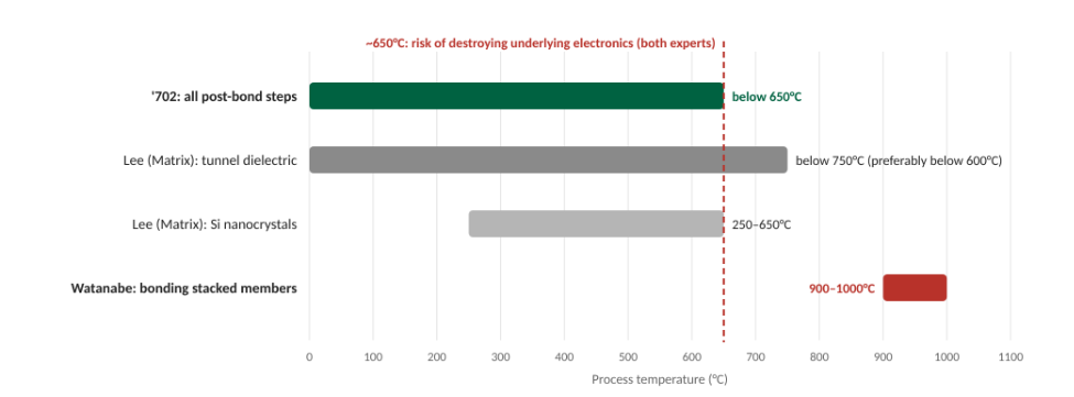
Figure 3: Process temperatures stated in each disclosure against the ~650°C damage threshold that experts for both sides gave the PTAB. Watanabe’s bonding sits 250–350°C above it.
5. How the ’702 structure differs from each reference
5.1 Watanabe: the right stack, made by a process that destroys it
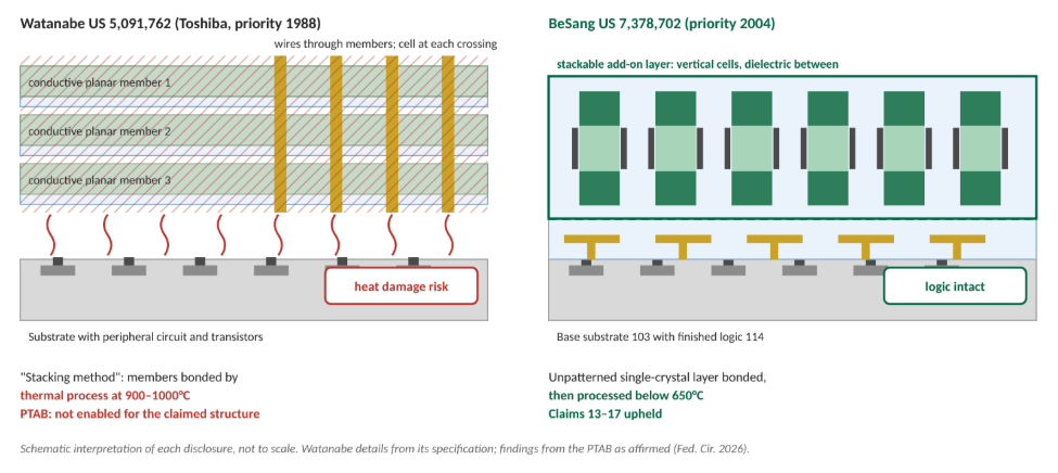
Figure 4: Watanabe bonds stacked members at 900–1000°C over a substrate carrying its peripheral circuit. The ’702 bonds an unpatterned single-crystal layer and keeps later steps below 650°C.
On paper, Watanabe has the architecture of claim 13: memory layers stacked over a substrate that carries devices. The difference is in how the stack is joined. Micron’s own expert testified that bonding above 650°C risks destroying the underlying electronic components (Micron J.A. 3632–34), and BeSang’s expert agreed (J.A. 3757–58). Watanabe’s 900–1000°C bonding therefore does not teach a skilled person how to make the claimed structure with working devices beneath it.
Point of comparison | Watanabe | ’702 |
Layer joined | Planar members, already wired | Unpatterned doped single-crystal layer |
Joining heat | 900–1000°C | Below 650°C after bonding |
Effect on substrate devices | Risk of destroying them (both experts) | Logic 114 and interconnect survive |
Where cells are defined | Before stacking | After bonding, by etching pillars |
Outcome | Not enabled; no reason to combine with the Lee Patent | Claims 13–17 upheld |
5.2 Lee Patent and Lee Application: deposited, not transferred
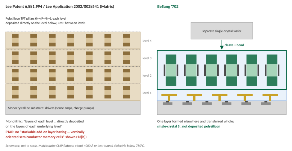
Figure 5: The Matrix disclosure builds each memory level by deposition directly on the level below. The ’702 forms a single-crystal layer elsewhere and transfers it whole.
Both Lee references come from the same Matrix Semiconductor application. Micron used the issued patent and Intel used the published application. Matrix calls its array “monolithic”: “layers of each level of the array were directly deposited on the layers of each underlying level.” It contrasts this with forming arrays separately and packaging them together. Its cells are thin-film transistors in amorphous or polycrystalline silicon.
The ’702 claims a “stackable add-on layer,” and its specification describes that layer as a cleaved, transferable, single-crystal portion of another wafer. The PTAB found that Intel had not shown the Lee Application teaches limitation 13[b], “a stackable add-on layer having a plurality of vertically oriented semiconductor memory cells.” Intel did not appeal that finding. Rightium observation: the drawings show why the difference is structural. A level deposited in place is not a layer that is made elsewhere and added on.
5.3 Park: dielectric between cells, but cells still connected
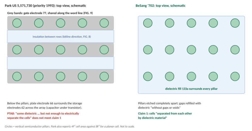
Figure 6: In Park, adjacent pillars share gate electrode 77 along the word line and sit above a common plate electrode 66. In the ’702, every pillar is surrounded by dielectric fill.
Park is closest to the ’702 at the cell level. It has vertical pillar transistors on an SOI-type bonded substrate, and it reduces DRAM cell area to 4F² against 8F² for a planar cell. But in Park’s FIGS. 8 and 9, adjoining cells “share[d] [a] plate electrode … and gate electrode,” with only “some dielectric material between the memory cells.”
The PTAB held that “the presence of some dielectric material between the memory cells, but not enough to electrically separate the cells from each other, [did] not meet the claim.” Intel did not dispute that reading of Park. Its argument that the PTAB had read in an “electrical separation” requirement was undercut by its own petition, which said the cells must be “electrically separated, as necessary for proper operations” (J.A. 554).
5.4 Kim: whole wafers stacked, not a layer patterned after transfer
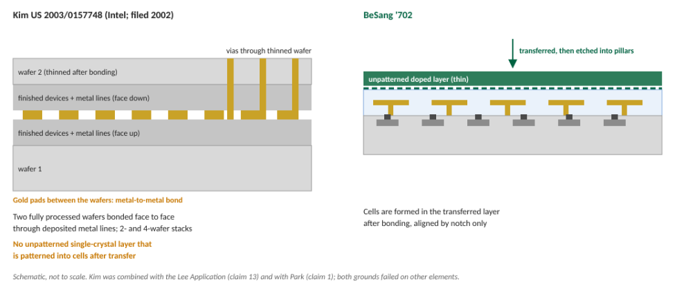
Figure 7: Kim bonds fully processed wafers face to face through metal lines and thins the top wafer. The ’702 transfers a thin unpatterned layer and forms its cells afterwards.
Kim, Intel’s own 2002 application, stacks finished wafers. Its devices are complete on each wafer before bonding, and the wafers are joined metal to metal. Intel paired Kim with the Lee Application for claim 13 and with Park for claim 1. Neither pairing reached Kim’s merits: the claim 13 grounds failed because 13[b] rested on the Lee Application alone, and the claim 1 ground failed on Park’s missing separation.
5.5 Aspar
Aspar, an article on a thin-film transfer process, supplied transfer technology in Intel’s second claim 13 ground. Intel’s petition did not rely on it for limitation 13[b], so the court did not reach it (footnote 2).
6. Claim map: every ground against every element
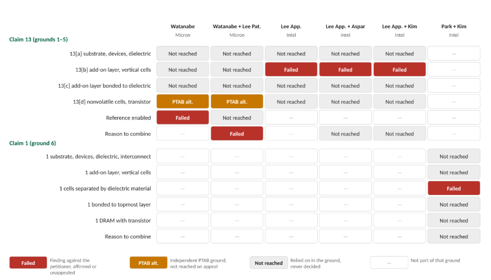
Figure 8: Outcome of each ground by claim element. Red cells are the findings that decided the case; grey cells were relied on but never decided.
6.1 Claim 13 chart
Element | What the petitioner relied on | Finding | Why |
13[a] substrate, devices, dielectric | Watanabe’s substrate with peripheral circuit; Lee’s substrate with drivers | Not decided | Grounds failed elsewhere |
13[b] add-on layer of vertical cells | Micron: Watanabe’s stacked members. Intel: the Lee Application only | Intel: not shown (unappealed) | Lee Application not shown to teach a stackable add-on layer; petition mapped no other reference |
13[c] add-on layer bonded to dielectric | Micron: Watanabe’s thermal bonding | Watanabe not enabled | 900–1000°C bonding risks destroying the substrate electronics; no other enabling evidence |
13[d] nonvolatile cells | Micron petition | PTAB: petition not directed to nonvolatile cells | Independent PTAB ground; not reached on appeal (fn. 1) |
Reason to combine (Watanabe + Lee Patent) | Improvement of Lee’s device | No motivation | Benefit outweighed by heat damage; improvement not explained |
6.2 Claim 1 chart
Element | What Intel relied on | Finding | Why |
Base with devices, dielectric, interconnect | Park + Kim | Not decided | Ground failed elsewhere |
Add-on layer of vertical cells | Park + Kim | Not decided | Ground failed elsewhere |
Cells “separated from each other by dielectric material” | Park FIGS. 8–9 | Not met | Cells share plate and gate electrodes; some dielectric does not separate them |
Bonded to topmost layer | Park + Kim | Not decided | Ground failed elsewhere |
DRAM with transistor | Park | Not decided | Ground failed elsewhere |
Findings are as described in the Federal Circuit opinion. Which reference Intel mapped to each undecided claim 1 element is not stated in the opinion, so those rows name the combination.
7. Why the court sided with the patent
Micron and Intel were the petitioners before the PTAB and the appellants on appeal, so they carried the burden of proving unpatentability throughout. The Federal Circuit affirmed because each failure rested on a PTAB fact finding supported by substantial evidence, or on the way the petitions were written.
Rule | Authority | Application |
Petitioner must prove unpatentability by a preponderance of the evidence | 35 U.S.C. § 316(e) | Each gap counted against the challengers |
Grounds and evidence must be stated with particularity | 35 U.S.C. § 312(a)(3) | Intel was held to its Lee-only mapping for 13[b] |
A reference relied on alone must enable the portion relied on | Raytheon v. GE, 993 F.3d 1374, 1380–81 (Fed. Cir. 2021) | Watanabe’s 900–1000°C bonding was not enabling |
A non-enabled reference with no other enabling evidence cannot render an invention obvious | Raytheon, 993 F.3d at 1377 | Micron offered no second source of a workable bond |
A fact finding from expert evidence is not claim construction | Google v. EcoFactor, 92 F.4th 1049, 1055 (Fed. Cir. 2024) | There was no hidden 650°C claim limit |
No specific improvement is required, but the rationale offered must hold up | Intel v. PACT XPP, 61 F.4th 1373, 1380–81 (Fed. Cir. 2023) | Micron’s improvement rationale was outweighed by heat damage |
The PTAB may read a petition as it is organised | Netflix v. DivX, 84 F.4th 1371, 1377 (Fed. Cir. 2023) | The 13[c] analysis did not rescue 13[b] |
Findings not appealed are forfeited | Bozeman v. Fed. Rsrv. Bank, 955 F.3d 971, 974 (Fed. Cir. 2020) | Intel left the Lee/13[b] finding unchallenged |
Fact findings are reviewed for substantial evidence | Consol. Edison v. NLRB, 305 U.S. 197, 229 (1938) | Testimony from both sides’ experts was enough |
7.1 The arguments that failed
- “The PTAB read a 650°C limit into claim 13.” Rejected. The PTAB found as a fact that Watanabe’s process does not work. It did not decide the claim’s scope.
- “A short burst stays within the thermal budget.” Rejected. The PTAB weighed time-and-temperature arguments against the expert evidence, and the court would not reweigh them.
- “The PTAB required proof of a specific improvement.” Rejected. The PTAB stated the correct law and answered the improvement rationale Micron itself advanced (J.A. 276–77).
- “The 13[c] analysis also covered 13[b].” Rejected. The petition relied only on the Lee Application for 13[b], under its own subheading.
- “The PTAB implicitly required electrical separation.” Rejected. The PTAB compared Park to the claim text, and Intel’s own petition had argued for electrical separation.
8. Why the invention was not obvious to a skilled person
Obviousness asks whether the claimed invention as a whole would have been obvious, at the time of the invention (June 2004), to a person of ordinary skill in the art. The Graham factors frame the inquiry: the scope and content of the prior art, the differences from the claims, and the level of skill. KSR permits flexible reasoning, but a challenger must still show a reason to combine and a reasonable expectation of success.
- The obstacle was the process, not the idea. Stacking was known (Watanabe, 1988). But the known way of joining layers, at 900–1000°C, would destroy the circuits underneath. A skilled person following Watanabe would end up with a damaged device.
- The ’702 contribution sits exactly at that obstacle. Doping before transfer, bonding an unpatterned single-crystal layer by notch alignment only, and keeping later steps below 650°C together make vertical cells possible over finished logic. No reference supplied that combination.
- Nearby art solved different problems. Matrix deposited polysilicon levels in place. Park built vertical DRAM with shared electrodes. Kim stacked whole finished wafers. None shows independent, dielectric-isolated vertical cells in a transferred single-crystal layer over logic.
- Hindsight is not a reason to combine. Micron’s combination asked a skilled person to accept device damage for an unexplained benefit, and the PTAB found no one would.
Strictly, the Federal Circuit held that the challengers failed to prove obviousness on the record they built, not that the invention was proven non-obvious. In an IPR the result for the patent owner is the same.
9. Lessons for attorneys: wording decided validity
9.1 For the drafter
- Claim the structure the hard step produces. The claims never recite 650°C. They recite a “stackable add-on layer” “bonded to” a substrate that already has “electrical devices formed therein.” Prior art that cannot make that structure without destroying the substrate is not enabled for it. A temperature limit would have been easy to design around; the structure is not.
- State the relationship, not just the location. “Separated from each other by dielectric material” is more than “with dielectric between them.” It defeated Park, whose cells had dielectric between them but shared electrodes.
- Use a defined term consistently. “Stackable add-on layer” appears in both independent claims and is backed by the description of a cleaved, unpatterned, transferable layer. That gave the PTAB a definite standard to compare deposited levels against.
- Write the process window into the specification. The patent’s “below 650° C” statements matched both experts’ damage threshold and anchored the finding that Watanabe was unworkable.
- Give each independent claim different fallbacks. Claim 1 relied on DRAM and dielectric separation. Claim 13 relied on nonvolatile cells and bonding to the dielectric layer. Dependent claims 14–17 added pillar-level detail.
9.2 For the challenger
- Prove the reference works. If the key reference’s process destroys the device, bring a second enabling reference or data. A thermal-budget theory needs time-and-temperature evidence, not argument.
- Map every reference to every limitation. Where a term repeats across limitations, address it in full under each one, or cross-reference expressly for each reference in each ground.
- Appeal the finding that hurts you. Intel’s unappealed 13[b] finding decided claim 13 by itself.
- Watch your own concessions. Positions taken to show motivation to combine (“electrically separated … to avoid shorts”) can define what a limitation requires.
9.3 The double edge
Words narrow enough to avoid the prior art can also be narrow enough to avoid infringement. In BeSang v. Micron (E.D. Tex. No. 2:23-cv-00028), the district court construed “stackable add-on layer” and entered judgment that the accused Micron SSDs (Crucial BX500, MX500, P3 Plus, P5 Plus; Micron 1100–2450 series) do not infringe. BeSang has appealed. The construction’s exact wording was not available in the source reviewed. The drafting goal is a structural term that is distinct from the prior art and still reads on the products competitors are expected to build, tested against both before filing.
Authorities and sources
- Micron Technology, Inc. v. BeSang Inc., Nos. 2025-1320, 2025-1377 (Fed. Cir. Oct. 30, 2026) (nonprecedential).
- Micron Tech., Inc. v. BeSang Inc., IPR2023-00900, 2024 WL 4765857 (P.T.A.B. Nov. 13, 2024); Intel Corp. v. BeSang Inc., IPR2023-00991, 2024 WL 5076376 (P.T.A.B. Dec. 11, 2024).
- Raytheon Techs. Corp. v. Gen. Elec. Co., 993 F.3d 1374 (Fed. Cir. 2021); Google LLC v. EcoFactor, Inc., 92 F.4th 1049 (Fed. Cir. 2024); Intel Corp. v. PACT XPP Schweiz AG, 61 F.4th 1373 (Fed. Cir. 2023); Netflix, Inc. v. DivX, LLC, 84 F.4th 1371 (Fed. Cir. 2023); Bozeman Fin. LLC v. Fed. Rsrv. Bank of Atlanta, 955 F.3d 971 (Fed. Cir. 2020); Consol. Edison Co. v. NLRB, 305 U.S. 197 (1938); Graham v. John Deere Co., 383 U.S. 1 (1966); KSR Int’l Co. v. Teleflex Inc., 550 U.S. 398 (2007).
- Patents (Google Patents): US 7,378,702 B2; US 5,091,762 A; US 6,881,994 B2; US 2002/0028541 A1; US 5,571,730 A; US 2003/0157748 A1.
- BeSang, Inc. v. Micron Technology, Inc., E.D. Tex. No. 2:23-cv-00028, case summary (PatSnap Eureka); BeSang press statement (StorageNewsletter, Mar. 13, 2023).
Editorial scope: Quotes from the PTAB decisions and the joint appendix (J.A.) are as reported in the Federal Circuit opinion. Prior-art descriptions come from the published specifications. All figures are Rightium schematics, not reproductions of patent drawings, and are not to scale. The Aspar article was not reviewed.
IP Research & Intelligence, Rightium